
Qualcomm says HBC memory chips pass tests for Dragonfly AI250
The company expects sampling during the first half of 2027, with specifications listing effective memory bandwidth of 133TB/s per card.
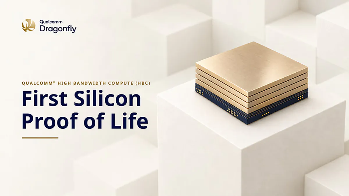
Qualcomm said testing of its initial High Bandwidth Compute (HBC) chips delivered the bandwidth and energy-efficiency gains it expected. The memory technology will power Dragonfly AI250, its accelerator for running artificial intelligence models in data centers.
The company's specifications give AI250 effective memory bandwidth of 133TB/s per card, 18 times the AI200 figure. Qualcomm cautioned that estimates comparing its technology with competitors are adjusted for target operating conditions. Performance in practice will vary with the finished hardware and the workload.
HBC puts computing functions near memory so data travels a shorter distance. Qualcomm says that arrangement improves effective bandwidth and computing output per watt, addressing constraints on data movement when operating large language models at scale.
At its San Diego laboratory, engineers used standard automated equipment to evaluate memory reading, writing and calculations near memory. They tested random data in sizes reflecting commercial products.
Separately, Qualcomm has sent a completed HBC data center design for manufacturing. Initial bring-up work has begun on a logic chip carrying directly bonded DRAM layers. Spare capacity and remapping functions allow the design to bypass defective memory cells.
AI250 will be included in Dragonfly Rack, a complete server rack intended for AI workloads. Qualcomm is targeting large enterprises, cloud providers and hyperscalers.